Homemade PCBs
Etching your own printed circuit boards is probably not a very sensible idea these days: many online services will do it for you for a reasonable cost, at pro quality. Still, when the need arises for a simple, 1-layer through-hole PCB to replace a messy protoboard with tons of wires, it is simple to do it yourself, and it’s quite fun. It does require a bit of equiment that is not cheap. Anyway, below are the steps I follow, there are many different ways to do this, this one works for me. It does involve some nasty chemicals, so gloves/protection goggles/throw-away clothes are recommanded, and you do this at your own (very limited) risk.
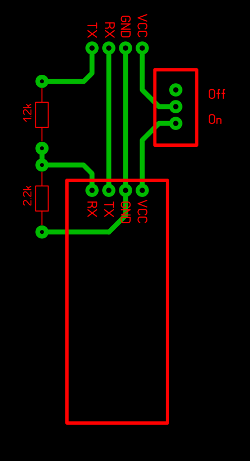
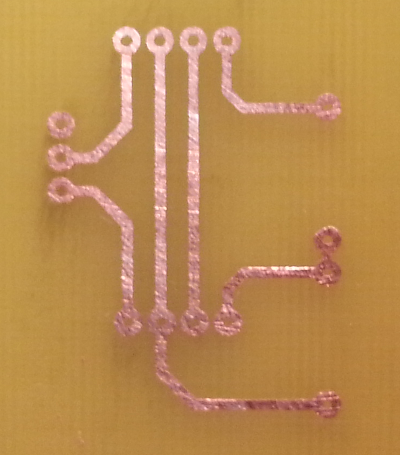
1) design the PCB using a layout software. EAGLE from CadSoft is clearly the gold standard, but I happen to use a much simpler (and much more limited) software: “Sprint Layout 6.0” from Abacom. It’s simple enough that I can focus on just getting the job done very rapidly, and rich enough that I have not yet outgrown it. Here is the layout I will be using for this example:
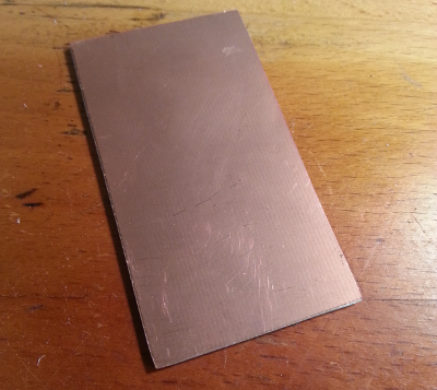
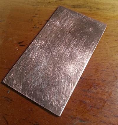
2) Get some copper clad boards. Cut a piece a bit larger than the size of the PCB you are designing
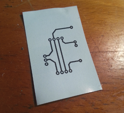
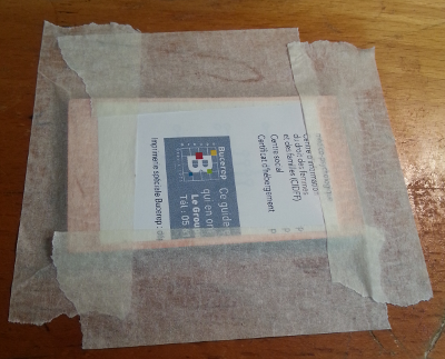
3) Print the layout, at scale 1:1, on glossy paper, using a laser printer (I got mine for 50 euros). I usually just use a page of the advertisement/magazines that come in the mail everyday, and it works fine. Cut the printed layout out of the page, leaving a margin on the borders.
4) Prepare the copper clad : use fine grain sanding paper or a scotch brite sponge to roughen the surface, then clean it with acetone, and avoid touching the surface afterwards
5) Place the printed layout against the copper clad, printed side against the copper, then place both on a surface that will withstand significant heat and can be damaged at will. I just use on old Ikea desk in my garage. Also, I use masking tape to hold the board in place.
6) And now for the main trick: a regular iron will be used to transfer the toner from the glossy paper onto the copper. Do get an old iron specifically for this, the iron sole will get stained over time.
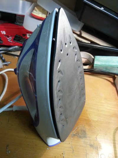
Plug the iron, set it to the maximum temperature, turn off vapor, and let it heat. Once it’s hot, carefully press the iron against the copper clad/paper assembly, and press very firmly, without moving. After a minute or so, start gently rotating the iron left and right, still applying as much pressure as you can, and continue like this for at least 5 minutes.
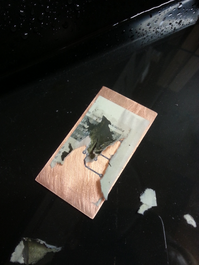
7) Pick-up the copper clad (with tweezers or something, it is still burning hot), put it in cold water and let it cool for a few minutes.
8) Gently peel-off the paper from the copper clad. I keep the copper clad underwater the whole time I am doing this, and rub the pulp of my finger on the paper until it starts to tear apart. It may take a while, but don’t rush it. After a while, the paper normally comes off easily:
9) once the paper is all gone, you should see black toner tracks on the copper clad, corresponding to your PCB layout. If anything looks unexpected (missing toner on a track somewhere, partially erased track), at this point you are better off restarting at step 4). A little acetone will easily clean the toner from the copper clad to restart from a fresh board.
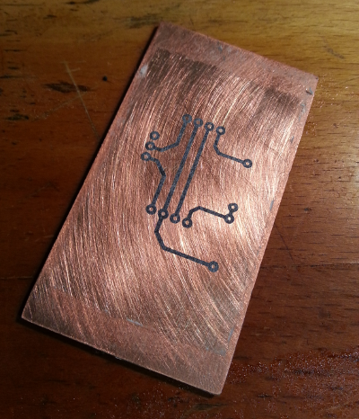
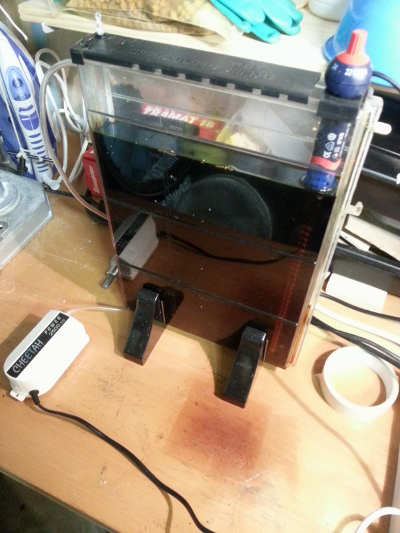
10) If the tracks are clean, it is time to etch. I use the oldschool way: Ferrite chloride, bought at an eletronics shop. Other more efficient etching chemicals exist, but they tend to be more dangerous to store & manipulate, whereas with ferrite chloride the worst than can happen is a pretty unremovable orange stain on your clothes. I bought a specific tank with a heater and an air pump to inject bubbles into the tank during etching. This speeds up the etching quite a bit, but just letting the copper clad soak in ferrite chloride works too, it only takes (much) longer.
I attach a couple of clamps to the board, to hold it while it will be inside the tank:
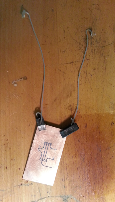
11) After about 5-6 minutes, I check the etching result. If it looks good, I rinse the copper clad with water. Notice the remains of copper where the clamps were masking the board during etching, just like the toner did.
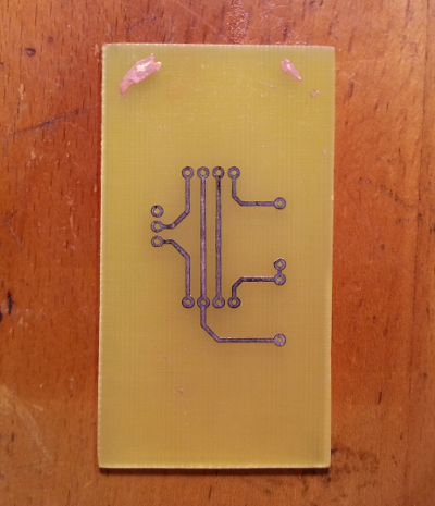
Then I clean the tracks with acetone to remove the toner. And Voilà !
12) An optional but useful step is tinning the resulting board, to prevent oxydation of the copper tracks and ease soldering. There are various ways to do this:
- a basic option is to just apply solder on the tracks, with a soldering iron. For anything except a very small/simple PCB, it takes forever and does not look too good in the end.
- the PCB can be soaked in a special liquid, creating a thin layer of tin on the tracks. I never had any repeatable success with this method, I must be missing something…
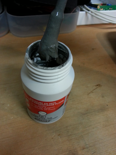
- I choose to use solder paste (tin+silver), easily found in any DIY store. A bit pricy, but a small bottle will last forever.
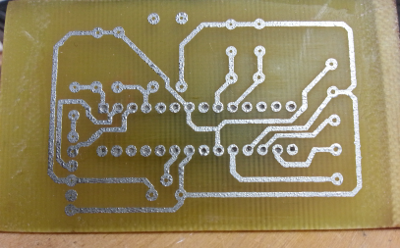
 I apply a thin layer of paste across all the PCB surface, with a small brush, and finally use a heat gun to melt the solder. The solder won’t stick on the epoxy, so it’s quite easy to remove it, leaving only the copper tracks covered with tin. And voila, not professional quality but decent and repeatable:
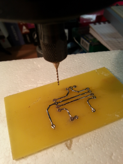
13) Time to drill the holes. This requires specific drill bits, since epoxy is quite a hard material and the drill diameters are very small. These can be bought in electronics shops, but be warned that they do tend to be expensive and fragile, you will break them from time to time. A drill press (or drill mounted on a vertical support) will make this quite straightforward.
14) For a complex PCB with many components, it is useful to print the top-side/silkscreen layout and imprint it on the non-copper-clad side of the board, using the iron. Place the components, solder them, cut the leads, and you are done.
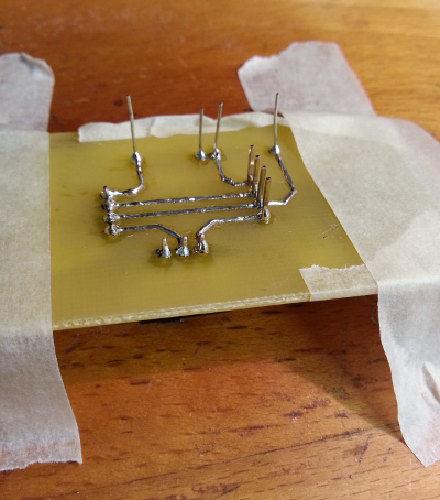
Of course the example PCB shown here is extremely simple (probably not worth a custom PCB in the first place…) but with the same technique, arbitrarily complex layouts with reasonably large tracks can be achieved. 2-layer PCBs can be done like this too, with the added difficulty of perfectly aligning both printed papers for toner transfer.